Front-End Semiconductor Engineering & Verification

VLSI Designs & Silicon Engineering

Complete front-end semiconductor workflows from synthesizable RTL microarchitecture and UVM testbench verification to logic synthesis, STA timing closure, and FPGA hardware emulation.

5nm & 7nm Ready
Advanced node design & closure
100% Coverage
UVM constrained-random closure
Industry EDA Flows
QuestaSim, ModelSim & Vivado

Production-Grade Front-End Engineering From Spec to GDSII

At VLSI Insights, we partner with semiconductor enterprises, fabless design startups, and research teams to execute front-end silicon development across complex modern nodes. Our engineering discipline spans synthesizable RTL authoring, multi-voltage clock and power domains, comprehensive UVM coverage closure, and rapid FPGA prototyping.

Whether you require turn-key IP subsystem integration, timing sign-off assistance, or automated regression setups, our senior designers ensure your microarchitecture is clean, lint-certified, and first-pass silicon-ready.

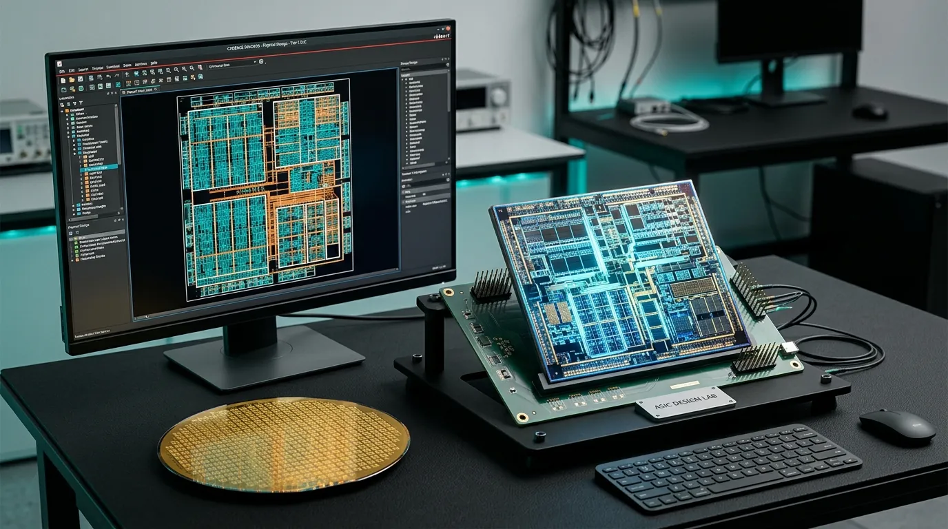
VLSI Front-End Silicon Design and Timing Analysis

Front-End Semiconductor Design Stack

We bridge high-level system requirements with synthesizable gate-level implementation through rigorous verification and timing compliance.

RTL Microarchitecture & Logic Design

Writing clean, synthesizable Verilog and SystemVerilog for high-throughput datapaths, FSM state controllers, memory arbiters, and standard on-chip buses (AXI/AHB/APB).

  • SystemVerilog IEEE 1800-2017 syntax
  • Clean SpyGlass lint and CDC compliance
  • Low power gating & architectural clock trees

UVM Functional Verification

Architecting modular, reusable Universal Verification Methodology (UVM 1.2) environments with constrained-random stimulus, SystemVerilog Assertions (SVA), and functional coverage closure.

  • Driver, monitor, scoreboard & sequencer flows
  • Corner-case bug isolation & bug tracking
  • 100% statement, branch & condition coverage

Synthesis & Static Timing Analysis (STA)

Mapping RTL to target foundry cell libraries, optimizing area/power/timing trade-offs, handling Multi-Corner Multi-Mode (MCMM) timing constraints, and closing setup & hold slacks.

  • Synopsys Design Compiler & Cadence Genus
  • SDC constraint generation & verification
  • Setup & hold slack zero-violation closure

FPGA Prototyping & Emulation

Real-time hardware verification on AMD Xilinx Artix-7, Kintex, and UltraScale+ platforms. Fast prototyping for firmware bring-up and pre-silicon validation before tape-out.

  • AMD Vivado & Intel Quartus toolflows
  • High-speed PCIe, DDR4, and Ethernet I/O interfaces
  • In-system hardware debugging with ILA cores

Low-Power Architecture & UPF

Multi-voltage domain design, power-gating architectures, retention flip-flops, level-shifters, and Unified Power Format (UPF / CPF) simulation verification.

  • Dynamic clock gating & operand isolation
  • Power-aware gate-level simulation
  • Leakage current minimization strategies

DFT & Scan Chain Insertion

Design for Testability integration including scan chain stitching, Boundary Scan (IEEE 1149.1 JTAG), Built-In Self-Test (BIST) for embedded memories, and ATPG test vectors.

  • Scan insertion & DRC rule checking
  • MBIST & Memory repair architectures
  • ATPG pattern generation with 99%+ fault coverage

Need Custom RTL Microarchitecture or Timing Closure?

From custom IP block microarchitecture to timing closure and multi-corner STA sign-off, our team brings battle-tested industry experience to accelerate your tape-out roadmap.

Request Technical Consultation

The Tape-Out Engineering Pipeline

How our engineering team takes chips from initial architectural specification to GDSII signoff.

Stage 01
Architecture
Microarchitecture specs, protocol partitioning, datapath budgeting & latency goals.
Stage 02
RTL & Lint
Synthesizable SystemVerilog, clean lint compliance, and clock-domain crossing design.
Stage 03
Simulation
UVM constrained-random testbenches, assertions (SVA), and 100% coverage closure.
Stage 04
Synthesis
Logic synthesis, SDC constraints mapping, and cell library mapping for area/power.
Stage 05
STA Closure
Static Timing Analysis, setup & hold slack optimization, and multi-corner timing closure.
Stage 06
Sign-Off
FPGA hardware emulation, netlist verification, DRC/LVS physical signoff, and GDSII handoff.

Schedule a VLSI Technical Consultation

Speak directly with our senior semiconductor engineers regarding RTL architecture, verification testbenches, or tool environment setups.