Industry-Calibrated Front-End Engineering Training

Technical Training & Career Pathways

Production-calibrated semiconductor engineering training tracks built by tape-out veterans. Hands-on Verilog RTL microarchitecture, SystemVerilog UVM functional verification, STA timing closure, and FPGA hardware emulation designed for undergraduates, career transitioners, and corporate teams.

100+ Hours Live Labs
QuestaSim, ModelSim & Vivado practice
Tier-1 Veteran Mentors
Decades of cumulative tape-out experience
100% Placement Support
Mock technical drills & recruiter drives

Bridging the Gap from Classroom to Silicon Floor

Traditional academic curricula teach theory, but semiconductor companies hire for practical tape-out competency. At VLSI Insights, our curriculum is engineered backward from actual job descriptions and recruitment benchmarks at leading semiconductor multinationals.

You write synthesizable RTL, debug real race conditions, build modular UVM testbenches from scratch, and synthesize circuits against standard cell foundry libraries. No generic slides — pure hands-on EDA engineering.

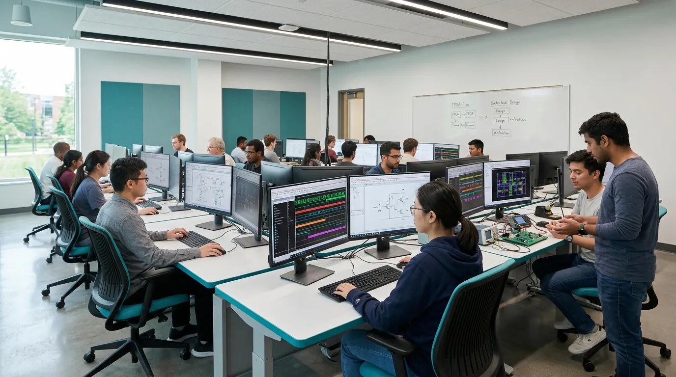
Technical Training Lab at VLSI Insights

Core Semiconductor Engineering Modules

Six comprehensive technical pillars covering every stage of front-end silicon development, verification, and hardware implementation.

RTL Microarchitecture & Synthesis

Mastering synthesizable Verilog and SystemVerilog for high-speed datapaths, FSM controllers, memory arbiters, and standard on-chip bus architectures.

  • SystemVerilog IEEE 1800-2017 syntax
  • SpyGlass linting & CDC compliance
  • Synthesis with Synopsys Design Compiler

SystemVerilog & UVM Verification

Architecting modular Universal Verification Methodology (UVM 1.2) environments with constrained-random stimulus, assertions (SVA), and coverage closure.

  • Driver, monitor, sequencer & scoreboard architecture
  • SystemVerilog Assertions (SVA) temporal checking
  • 100% statement, branch & functional cross-coverage

FPGA Emulation & Hardware Bring-Up

Implementing RTL designs on AMD Xilinx Artix-7 and Kintex platforms. Handling pin mapping, timing constraints, and hardware debugging with integrated logic analyzers.

  • AMD Vivado & Intel Quartus workflows
  • Hardware debugging using Integrated Logic Analyzer (ILA)
  • High-speed peripheral interfacing (SPI, UART, AXI)

Static Timing Analysis & SDC Closure

Understanding setup and hold slack calculations, clock jitter, skew, Multi-Corner Multi-Mode (MCMM) timing constraints, and logic equivalence checking.

  • Synopsys PrimeTime timing closure
  • SDC generation, false paths & multi-cycle paths
  • Formal Logic Equivalence Checking (LEC)

Embedded Firmware & Silicon Bring-Up

Bridging silicon registers with production code using bare-metal C and FreeRTOS task scheduling across ARM Cortex-M and RISC-V architectures.

  • Low-level peripheral driver writing (I2C, SPI, CAN)
  • RTOS deterministic preemption & ISR routines
  • JTAG / SWD in-circuit board diagnostics

Interview Drills & Tape-Out Portfolio

Rigorous 1-on-1 mock technical interviews, waveform bug-hunt challenges, resume crafting tailored to semiconductor recruiters, and placement drives.

  • Whiteboard architecture & timing diagram drills
  • Industry project portfolio on GitHub & paper summaries
  • Direct recruitment referrals to partner companies

Full Program Curriculum & Batch Schedules

Detailed syllabus PDFs, weekend vs. weekday timings, lab reservation credentials, and scholarship opportunities are available. Speak directly with our admissions team.

Explore All Programs Talk to Admissions

The Engineering Mastery Roadmap

How our immersive learning tracks transform aspiring engineers into tape-out ready semiconductor professionals.

Stage 01
Digital Specs
Boolean logic, timing budgets, micro-architecture specifications, and datapath block diagrams.
Stage 02
RTL & Linting
Synthesizable Verilog/SystemVerilog, SpyGlass lint rules, and CDC clock domain crossing sanity.
Stage 03
UVM Testbench
Architecting UVM 1.2 agents, constrained-random stimulus, scoreboards, and SVA assertions.
Stage 04
Synthesis & STA
Gate-level mapping with Synopsys DC, SDC timing constraints, and setup/hold slack zero closure.
Stage 05
FPGA Prototype
AMD Vivado implementation, hardware flashing, oscilloscope probing, and ILA core debug.
Stage 06
Recruitment Drive
Mock technical interviews, corporate recruitment matching, and technical offer sign-off.

Schedule a Technical Training Consultation

Speak directly with our senior instructors and coordinators regarding batch schedules, eligibility, lab access, and placement assistance.