VLSI Related Services
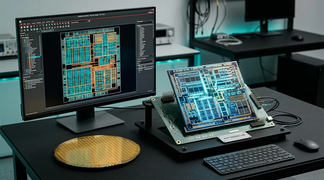
Production-grade semiconductor engineering from RTL microarchitecture and UVM functional verification to synthesis, STA timing closure, and FPGA hardware emulation.
Explore VLSI Designs
Specialized front-end VLSI chip design, technical engineering training, and targeted digital solutions. Built to bridge classroom theory and production silicon execution.

Specialized Semiconductor Practices
From silicon front-end architecture and verification to intelligent edge models and digital growth services, we empower engineering minds and technology enterprises.
Production-grade semiconductor engineering from RTL microarchitecture and UVM functional verification to synthesis, STA timing closure, and FPGA hardware emulation.
Explore VLSI DesignsConstrained-random testbenches, assertions (SVA), coverage closure, and regression management for multi-million gate ASICs.
Explore SOC VerificationBare-metal firmware, FreeRTOS architectures, hardware drivers, and board bring-up across ARM Cortex-M, ESP32, and RISC-V platforms.
Explore EmbeddedQuantized neural network deployment, TinyML edge inference, and hardware-accelerated computer vision models for microcontrollers and FPGA.
Explore AI ModelsTargeted digital marketing, IVR telephony systems, and managed communication operations for electronics companies and technical brands.
Explore Marketing SolutionsModern, responsive web applications, engineering portals, student learning platforms, and high-conversion landing pages built for scale.
Explore Web DevTraining Programs & Certifications
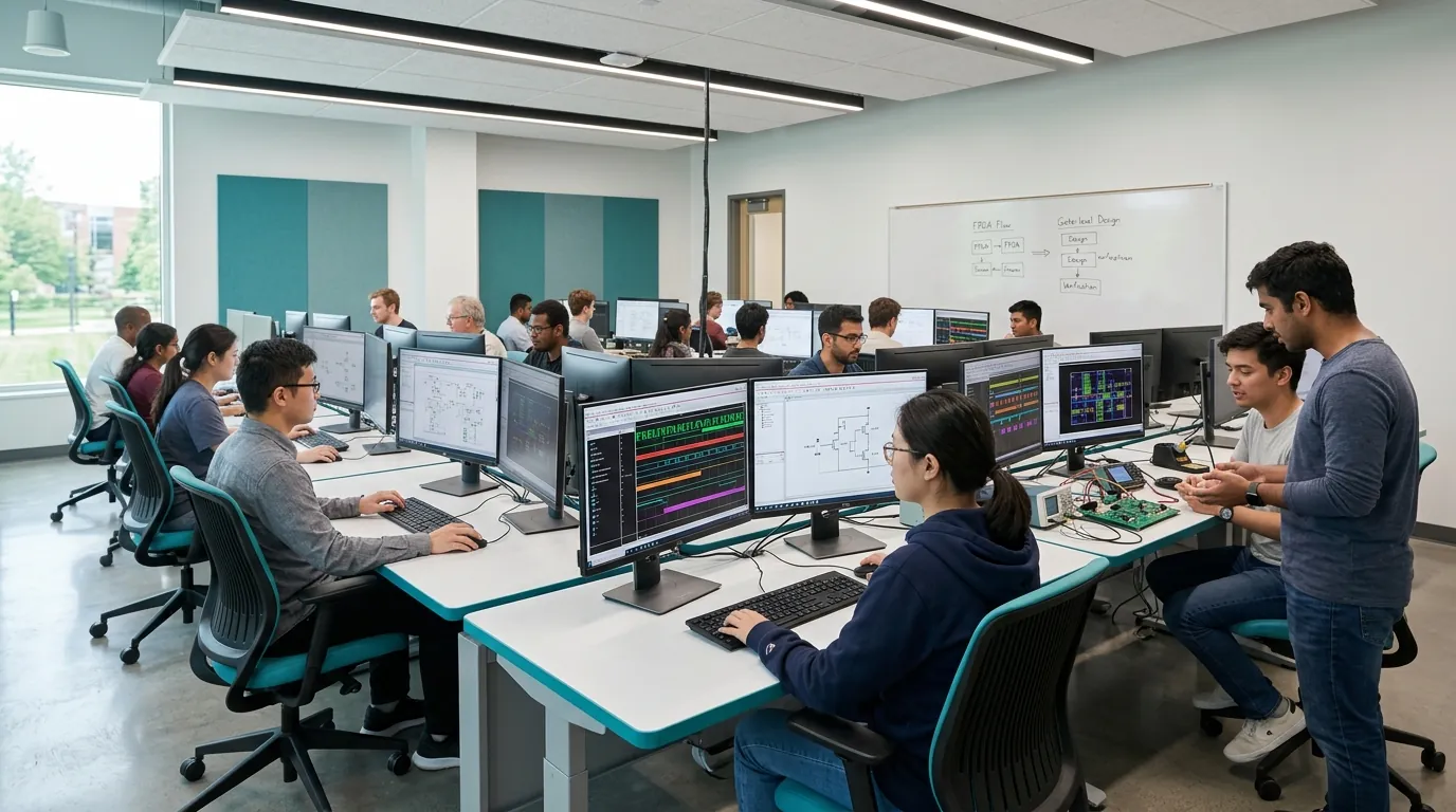
Practical, structured training programs designed to take you from beginner to job-ready, whether you're a college student or a working professional.
Start from zero and get placed in a top semiconductor company in 16 weeks, with personal mentor support throughout.
For working engineers who want to master the most advanced steps in bringing a chip to market: faster and with fewer errors.
Production Tape-Out Methodology
Learn directly from senior tape-out engineers with decades of combined experience across global semiconductor leaders.
Work on real SoC architectures, SystemVerilog/UVM testbenches, and physical design timing closure - not toy academic exercises.
Direct referral pipeline, technical interview drills, and resume vetting tailored to semiconductor hiring expectations.
Industry Alumni in Production
"The training gave me exactly the practical skills I needed to crack the technical interview rounds at a top semiconductor company."
"Here we worked on real chip designs, not just college textbook problems. The mentor guidance throughout the program was incredibly valuable."
"The hands-on projects and real-world assignments gave me the confidence to work on large, complex chip verification tasks from day one."
"Learning scripting and automation alongside chip design gave me a big advantage. My interview at Cadence went smoothly thanks to this training."
"The practical experience on advanced chip design helped me transition smoothly from a student into a real industry production team at ARM."
"Everything we practiced in training mapped directly to the questions I was asked during my campus placement interviews. I felt fully prepared."
"The floorplanning, CTS, and routing congestion modules gave me hands-on confidence to solve actual physical design challenges in complex SoC blocks."
"Writing SystemVerilog assertions and architecting functional coverage groups prepared me directly for multi-round semiconductor interviews."
"The depth of timing closure and synthesis constraint analysis was remarkable. I learned design best practices that usually take years on the job."
"Transitioning from generic academic simulations to tape-out ready industry EDA workflows was the defining turning point in my VLSI career."
"Building complete UVM testbenches with scoreboards and checkers gave me the exact skills that my hiring manager was specifically looking for."
"Hands-on board bring-up and FPGA prototyping labs made all the difference. Learning register maps and bus protocols was invaluable."
*Logos and company trademarks are the property of their respective owners.
Our engineers are actively recruited by the world's foremost semiconductor design teams, fabless innovators, and EDA software leaders.
Reach out for program enquiries, academic partnership discussions, corporate training engagements, or consultation on any of our technical services.
Thank you for reaching out to VLSI Insights. Our engineering coordinator will connect with you shortly.